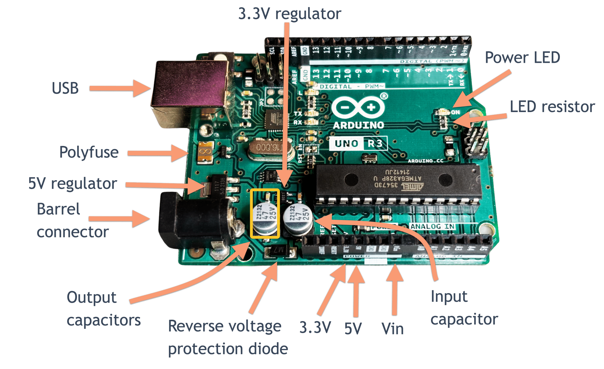
The Ultimate Guide To Optimizing Your Arduino Pcb Layout For Improved Signal Integrity And Reduced Electrical Noise - Pin layout of arduino uno pcb circuits
If you are searching about What Are the Different Types of Arduino PCB Design, and How Do They you've came to the right place. We have 35 Images about What Are the Different Types of Arduino PCB Design, and How Do They like Local PCB Layout Tweaks for Improved Signal Integrity When Using ESD, Optimizing Signal Integrity in RF PCB Layout: Best Practices and also Schematic diagram and PCB design - General Guidance - Arduino Forum. Read more:
What Are The Different Types Of Arduino PCB Design, And How Do They
 hillmancurtis.com
What Are the Different Types of Arduino PCB Design, and How Do They ...
High-Speed PCB Signal Integrity Design Tutorial - TechSparks
 www.tech-sparks.com
High-Speed PCB Signal Integrity Design Tutorial - TechSparks
Schematic Layout: PCB Geometry, Parasitics, And Signal, 51% OFF
Schematic Layout: PCB Geometry, Parasitics, And Signal, 51% OFF
Arduino Uno Layout Pcb Circuit Boards
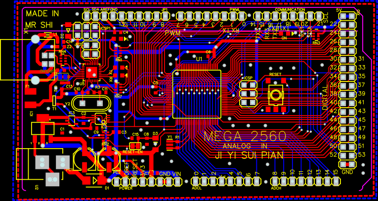 narodnatribuna.info
Arduino Uno Layout Pcb Circuit Boards
G.SKILL Unveils Newly Enhanced DDR5 R-DIMM Memory With 16-Layer PCB For
 www.msn.com
G.SKILL Unveils Newly Enhanced DDR5 R-DIMM Memory with 16-Layer PCB for ...
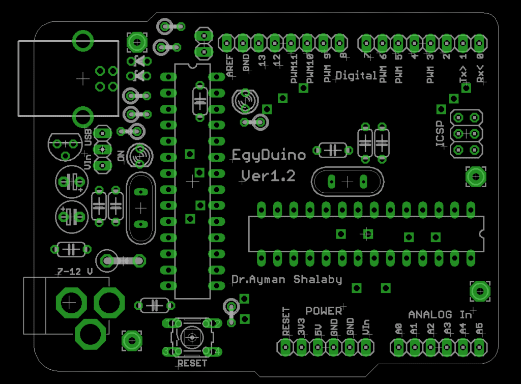
Pin Layout Of Arduino Uno Pcb Circuits
 narodnatribuna.info
Pin Layout Of Arduino Uno Pcb Circuits
Signal Integrity Analysis | PCB Signal Integrity Solutions – GigHz
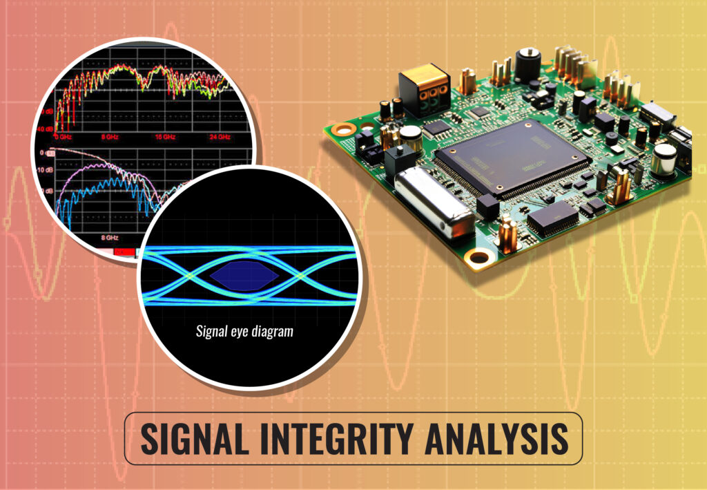 gighz.net
Signal Integrity Analysis | PCB Signal Integrity Solutions – GigHz
Optimizing Signal Integrity In Multi-board PCB Systems
 vyaparpages.com
Optimizing Signal Integrity in Multi-board PCB Systems
How PCB Dielectric Materials Impact High-Speed Signal Integrity: Rise
 www.fastturnpcbs.com
How PCB Dielectric Materials Impact High-Speed Signal Integrity: Rise ...
5: Measure Of The Electrical Noise Of The Recording Setup And Improved
 www.researchgate.net
5: Measure of the electrical noise of the recording setup and improved ...
Optimizing PCB Layout For Assembly And Manufacturing Efficiency
 microcad3d.com
Optimizing PCB layout for assembly and manufacturing efficiency
Hermetic Seal Male PCB Mount Limited Detent RF Connector Improved
 www.rf-coaxialconnector.com
Hermetic Seal Male PCB Mount Limited Detent RF Connector Improved ...
Signal Integrity In PCB: Issuses And Proven Design Solutions
 www.elepcb.com
Signal Integrity in PCB: Issuses and Proven Design Solutions
PCB Signal Integrity: Factors, Design Tips, And Testing Methods
 www.mokotechnology.com
PCB Signal Integrity: Factors, Design Tips, and Testing Methods
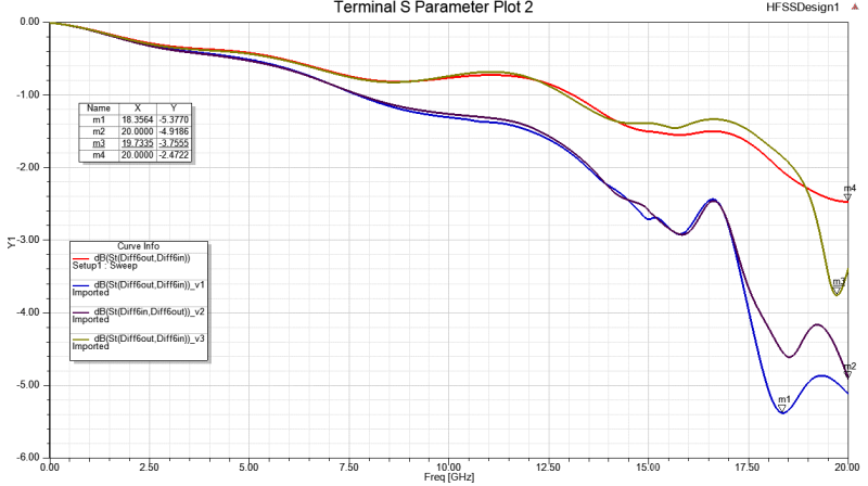
Optimizing Signal Integrity In RF PCB Layout: Best Practices
 jamindopcba.com
Optimizing Signal Integrity in RF PCB Layout: Best Practices
Arduino Nano Pcb Layout – Arduino Microcontroller Circuit Diagram – DYAX
 hoo.empirestatehealthsolutions.com
Arduino Nano Pcb Layout – Arduino Microcontroller Circuit Diagram – DYAX
Maximizing High-Speed Signal Integrity: Advanced PCB Layout Techniques
 86pcb.com
Maximizing High-Speed Signal Integrity: Advanced PCB Layout Techniques ...
How To Optimize PCB Layout For Signal Integrity | RunTime
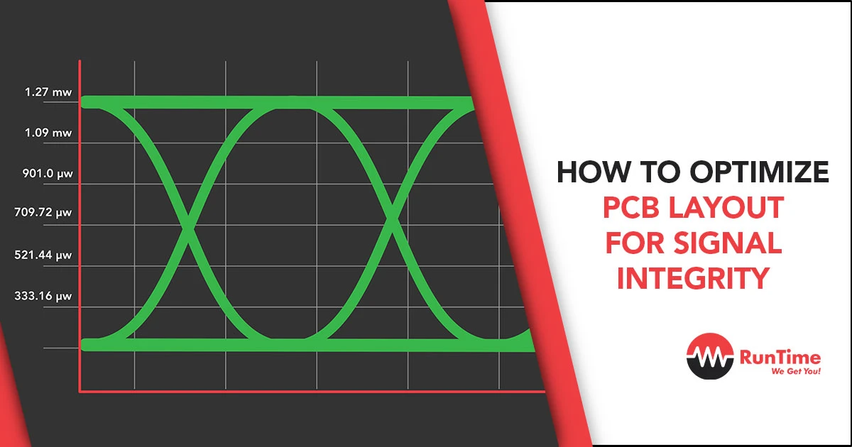 runtimerec.com
How to Optimize PCB Layout for Signal Integrity | RunTime
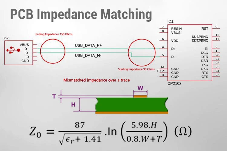
SMA Connector PCB Layout: Best Practices For Optimal Signal Integrity
 hillmancurtis.com
SMA Connector PCB Layout: Best Practices for Optimal Signal Integrity ...
Pre-layout Work And Good Signal Integrity Simulation - Radientum
 www.radientum.com
Pre-layout work and good signal integrity simulation - Radientum
Local PCB Layout Tweaks For Improved Signal Integrity When Using ESD
 incompliancemag.com
Local PCB Layout Tweaks for Improved Signal Integrity When Using ESD ...
Schematic Diagram And PCB Design - General Guidance - Arduino Forum
 forum.arduino.cc
Schematic diagram and PCB design - General Guidance - Arduino Forum
Pin Diagram Arduino Uno Pinout Pcb Circuits
 narodnatribuna.info
Pin Diagram Arduino Uno Pinout Pcb Circuits
PCB Signal Integrity : Mixing Up The Signals In The Right Way - IBE
 www.pcbaaa.com
PCB signal integrity : mixing up the signals in the right way - IBE ...
Optimizing PCB Layout For Performance And Reliability: Best Practices
 iies.in
Optimizing PCB Layout for Performance and Reliability: Best Practices ...
PCB Impedance Testing: Why It Matters For Signal Integrity
 www.allpcb.com
PCB Impedance Testing: Why It Matters for Signal Integrity
Basic Circuit Diagram Pcb Layout
 www.circuitdiagram.co
Basic Circuit Diagram Pcb Layout
Embedded Passive Component Pcbs For Space-Saving And Improved Signal
 lctech-pcb.en.made-in-china.com
Embedded Passive Component Pcbs for Space-Saving and Improved Signal ...
Enhancing Signal Integrity In PCB Design: Key Considerations And
 resources.altium.com
Enhancing Signal Integrity in PCB Design: Key Considerations and ...
Multi-Board PCB Signal Integrity: A Complete Guide
 resources.altium.com
Multi-Board PCB Signal Integrity: A Complete Guide
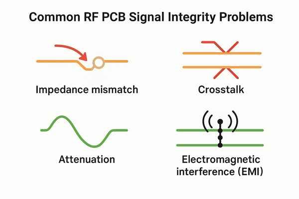
What Key Actions Solve Common RF PCB Signal Integrity Issues
 magellancircuits.com
What Key Actions Solve Common RF PCB Signal Integrity Issues ...
Arduino Pcb Schematic » Diagram Board
 www.diagramboard.com
Arduino Pcb Schematic » Diagram Board
Optimizing PCB Layout For HV CoolGaN™ Power Transistors - White Paper
 www.allaboutcircuits.com
Optimizing PCB Layout for HV CoolGaN™ Power Transistors - White Paper
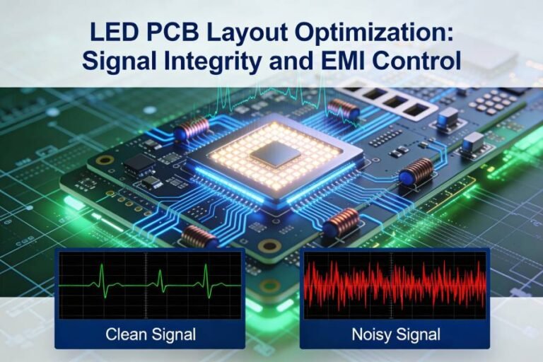
LED PCB Layout Optimization: Signal Integrity & EMI Control Guide - JHYPCB
 www.pcbelec.com
LED PCB Layout Optimization: Signal Integrity & EMI Control Guide - JHYPCB
How To Improve Signal Integrity In PCB Design (Guidelines) - Artist 3D
 artist-3d.com
How to Improve Signal Integrity in PCB Design (Guidelines) - Artist 3D
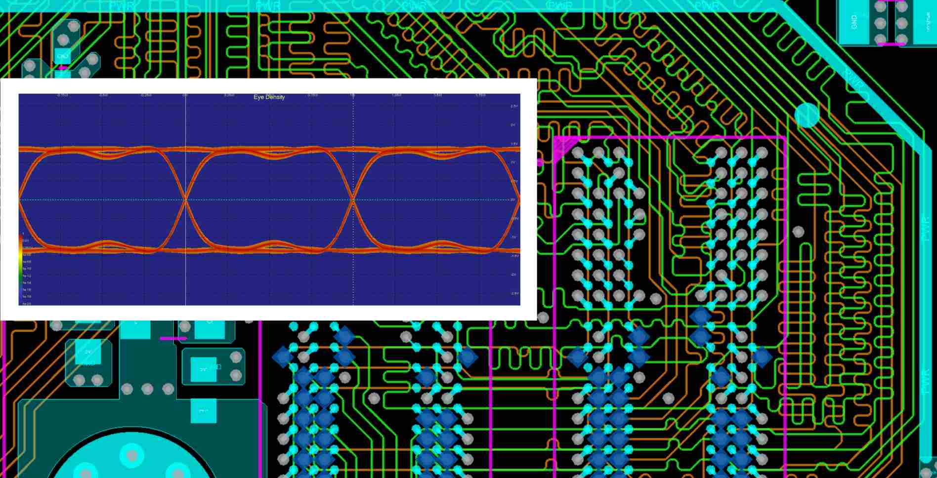
Signal integrity analysis. pcb impedance testing: why it matters for signal integrity. G.skill unveils newly enhanced ddr5 r-dimm memory with 16-layer pcb for